Curve CMOS Imaging Sensors at industrial scale
SILINA, a deeptech startup in microelectronics, has brought new technology to the imaging industry by curving the imaging sensors. Curved sensor technology is being developed for many years but was limited to single-chip manufacturing processes, until now.
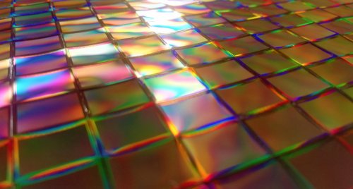
SILINA has been developing a technology which enables to curve hundreds of imaging sensors at the same time, offering new perspectives in the design of cameras, from high volume to niche markets.
In nature, most vision systems use curved retinas, like human eyes. Curved retinas enable to use simple optical lens with only one lens, the crystalline, providing a wide field of view for an outstanding image quality, making the eyes very compact.
Unfortunately, all electronic imaging systems use flat imaging sensors which require making the lens very complex, using many expensive optical elements. This degrades the optical performance and capabilities of the camera, and increases the mass/volume budget and overall cost of any camera and optical system.
Curved imaging sensor technology is the next major innovation for the imaging industry. It disrupts the way vision systems are designed. It overcomes hardware limitations that no software can solve and enable a whole new generation of cameras. It provides drastic improvements on four key criteria: increased image quality and detection capability, and reduced cost and bulk of cameras.
An innovative process for scaling
Wilfried JAHN, CTO and co-founder of SILINA, has been developing and optimizing a curving process with the objective to scale and reach high volume markets. He explained: “Our innovation has been driven to unlock the technological barriers of scalability. Previously, this technology was limited to niche markets since the various solutions were limited to manual single-chip manufacturing processes, delivering a few tens of units during the past 20 years.
“Thanks to cross-pollination ideation of various professional experiences, we have been able to create a unique process to curve hundreds chips at the same time. We can control all the parameters which make the process reliable and repeatable, reducing significantly the cost of production. One month after creating SILINA, we have curved 275 units of one-inch CMOS imaging sensors at the same time, a world first demonstration.”
SILINA’s curving process is the same whatever the sensor format and technology, notably CMOS and CCD. It can be applied to Front-Side Illuminated (FSI), Back-Side Illuminated (BSI) sensors, and on various spectral bandwidths from ultraviolet, visible to infrared. This process enables low volume and high volume manufacturing, curving one sensor, several sensors or a full wafer at a time. Also, various shapes can be obtained: spherical, aspherical, freeform and custom shape on-demand.
This manufacturing process has also been developed to keep the same original packaging used for classic flat sensors, meaning that the mechanical architecture and electronic board remain the same, facilitating the integration of the technology on current production lines.
A dual business model
Michaël BAILLY, CEO and co-founder of SILINA, detail the startup said: “Our services are offered to optical system designers and manufacturers, camera integrators and sensor manufacturers to support them in the improvement of their imaging system performance while reducing their cost of production. Our offer is made of two propositions, a support in optical system design to integrate the curved sensor technology in their specific applications, and an on-demand service to curve their imaging sensors. SILINA does not design nor manufactured its own sensors, but curve existing flat sensors. Finally, we plan to reach high volume markets via IP licensing.”
SILINA’s technology brings a significant benefit for the imaging industries: aerospace, defense, photography, automotive, smartphone and others.
The main value proposition is specific to each market segment and application: e.g. high image quality for smartphones, low mass/volume budget for aerospace and drones, better detection capability for automotive. Michael BAILLY continued: “These needs drive our technological developments in several complementary aspects including yield of production, shape accuracy and resistance to environmental constraints. In the end, each technological development for a specific application benefits the others.
“Microelectronics and photonics projects are defined by the European Commission as Important Projects of Common European Interest. Curved imaging sensor technology complies with this scope. It’s a real asset for European companies, and SILINA will deliver it at large scale.”

