Metamaterial Lenses Target Consumer Electronics
Refractive lenses have been around forever—800 years, in fact. The basic architecture of lenses, however, may be changing.
Metamaterials could revolutionize lensing systems. Conventional lenses rely on refraction at interfaces to focus light. In comparison, metamaterial lenses use a finely patterned surface to vary the effective refractive index across the lens. This introduces phase variation and changes the direction of the light via interference. Metalenses can be made from silicon wafers using highly scalable lithography processes. They could also enable simpler supply chains as tech can simultaneously produce lens and image sensors.

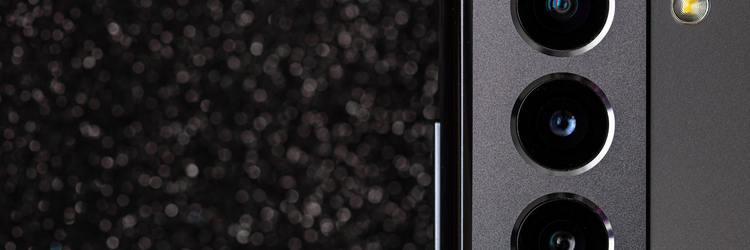
Instead of being curved, metalenses can be flat, reducing the weight and size of the lens housing and eliminating the “camera bulge” common to smartphones. This will mean a reduction in cost due to integrated manufacturing and additional product differentiation in an increasingly homogenous smartphone market.
Use cases go beyond consumer electronics. Compatibility with time-of-flight depth sensors, metalenses can be integrated with LiDAR systems for AVs and robots and be used with dot projection systems for facial recognition.
Technical challenges still exist and the biggest difficulty is overcoming chromatic aberration where different wavelengths of light are focused onto different points, leading to a blurry full-color image.
The IDTechEx report, “Metamaterials Markets 2023-2043: Optical and Radio-Frequency”, discusses the potential of metalenses.

