New ultra-small devices are ideal for rapid charging applications
Toshiba Electronics Europe has announced the launch of two new N-channel MOSFET drivers suitable for rapid-charging and other high current applications.
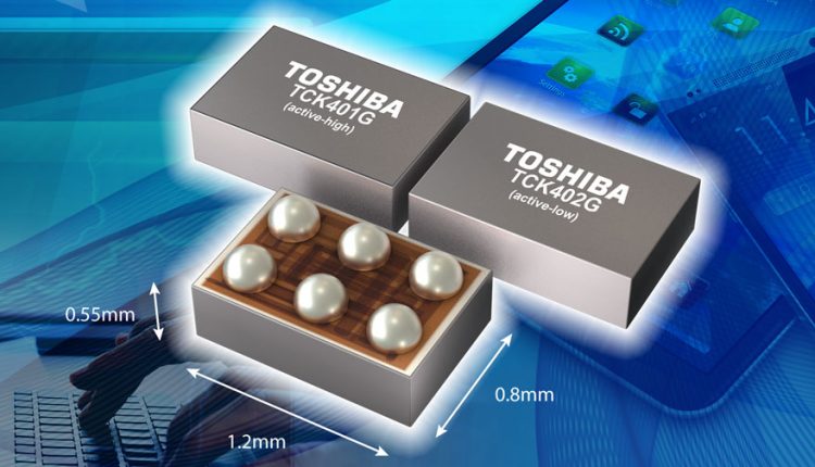
The new TCK401G (active-high) and TCK402G (active-low) charge pump driver ICs are suitable for high current mobile charging applications when used in conjunction with low RDS(on) N-channel MOSFETs. The driver ICs support several built-in safety functions, including overvoltage protection, inrush current reduction and auto output discharge.
Operating from an input voltage in the range 2.7 to 28VDC, the devices draw just 121μA of quiescent current (IQ). Switching times for the gate voltage (VGATE) are 0.58ms (ON) and 16.6μs (OFF).
A high-efficiency power supply circuit can be realized by using one of the new drivers with one or two external N-channel MOSFETs that have a maximum voltage rating and on-resistance suitable for the intended application. As an example, the combination of a TCK40xG driver IC and the low on-resistance SSM6K513NU MOSFET is ideal for mobile or consumer applications, as it makes it possible to build a 100W power supply with a very compact footprint.
Even with the high level of integration, the driver ICs are still housed in the small industry-leading WCSP6E package, measuring just 0.8×1.2×0.55mm.
Volume shipment of the new MOSFET driver ICs has started.

