Ninety-seven IC wafer fabs closed or repurposed in past ten years
The IC industry has been on a mission to pare down older capacity (≤200mm wafers) in order to produce devices more cost-effectively on larger wafers. In its recently released Global Wafer Capacity 2019-2023 report, IC Insights shows that due to the surge of merger and acquisition activity in the middle of this decade and with more companies producing IC devices on sub-20nm process technology, suppliers are eliminating inefficient wafer fabs.
Over the past ten years (2009-2018), semiconductor manufacturers around the world have closed or repurposed 97 wafer fabs, according to findings in the new report.
The graph below shows that since 2009, 42 150mm wafer fabs and 24 200mm wafer fabs have been shuttered. Also, 300mm wafer fabs have accounted for only ten percent of total fab closures since 2009. Qimonda was the first company to close a 300mm wafer fab after it went out of business in early 2009.
 Three 150mm wafer fabs were closed or repurposed in 2018. Two of these fabs belonged to Renesas. Renesas closed one fab in Konan, Kochi, Japan that produced analog, logic, and some older microcomponent devices. A second Renesas fab in Otsu, Shiga, Japan was repurposed and now makes only optoelectronic devices. A third fab, Fab 1 belonging to Polar Semiconductor (now Sanken) in Bloomington, Minnesota, also was closed. This fab manufactured analog, discretes, and offered some foundry services.
Given the skyrocketing cost of new wafer fabs and manufacturing equipment, and as more IC companies transition to a fab-lite or fabless business model, IC Insights anticipates there will be additional fab closures in the next few years. Five closures/repurposed fabs have already been publicly announced. Samsung’s 300mm memory fab (Line 13) will be fully converted this year to produce image sensors and TI’s 200mm analog GFAB in Greenock, Scotland, is expected to close by June 2019. Renesas plans to close two 150mm fabs (Otsu, Shiga and Ube, Yamaguchi, Japan) in 2020 or 2021, and Analog Devices plans to close its 150mm wafer fab in Milpitas, California in February 2021.
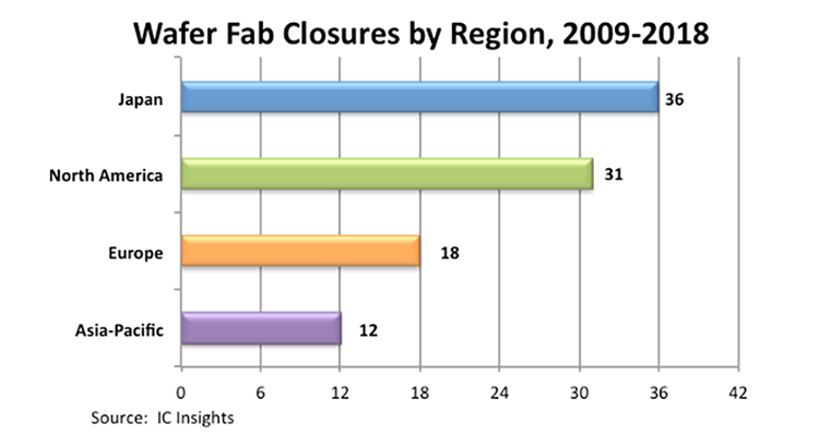
Semiconductor suppliers in Japan have closed a total of 36 wafer fabs since 2009, more than any other country/region. In the same period, 31 fabs were closed in North America, 18 fabs were shuttered in Europe, and 12 wafer fabs were closed throughout the Asia-Pacific region. With 36 fab closures and very few new fabs going up there, it is little wonder that Japan now accounts for only 5% of worldwide semiconductor capital spending.
Report details: Global Wafer Capacity 2019-2023
IC Insights’ ‘Global Wafer Capacity 2019-2023—Detailed Analysis and Forecast of the IC Industry’s Wafer Fab Capacity’ report assesses the IC industry’s capacity by wafer size, minimum process geometry, technology type, geographic region, and device type through 2023. The report includes detailed profiles of the companies with the greatest fab capacity and gives comprehensive specifications on existing wafer fab facilities.
Global Wafer Capacity 2019-2023 is priced at $4,890 for an individual user license. A multi-user worldwide corporate license is available for $7,590.


