The building blocks of photonic devices inside of silicon
When a laser beam modifies a material, those modifications can either be temporary or permanent, and the change can also be either extremely subtle or drastic. In any case, once such a modification has taken place, the modified material starts responding differently to the laser beam.
This interaction between the laser beam and the modified materials is typically overlooked or even actively prevented because it’s viewed as an undesired artifact. However, researchers at Bilkent University and Middle East Technical University (both in Ankara, Turkey) have taken advantage of these interactions to create structures within silicon that enable photonic devices.
In research described in the journal Nature Photonics, the Turkey-based researchers have developed a 3D laser fabrication technique that deliberately creates the conditions for exploiting these interactions, known as nonlinear feedback mechanisms. The researchers have dubbed the resulting structures inside of the silicon ‘in-chip’ devices that they believe can serve in a host of applications. Among the predicted uses: silicon-based photonics components for near- and mid-IR photonics.

“In order to differentiate these elements from their “on-chip” counterparts, we have coined the term “in-chip,” explained Onur Tokel, an assistant professor at Bilkent who was the lead author of the paper.
“So far, the field of silicon-photonics has occupied itself primarily with on-chip photonics, which has been fantastically successful. We now envision and demonstrate proof-of-concept silicon-photonics in-chip elements to complement these.”
To arrive at their new 3D laser fabrication technique, the Tokel and his colleagues Serim Ilday and Fatih Omer Ilday looked specifically at what conditions would allow a positive feedback loop between modifications of the material and the corresponding effect on the laser beam (its absorption, scattering, diffraction, focusing, etc.).
Tokel and his colleagues used nanosecond lasers that have existed for more than a decade.
When a positive feedback is set up, it becomes possible for even subtle changes to build up iteratively, rapidly, and often exponentially. After the changes cross a certain threshold, the modification in the material becomes permanent. So, the key to the researchers’ approach is to exploit nonlinearities in the form of positive feedback loops, according to Tokel.
In the approach adopted by Tokel and his colleagues, thermal energy is built up on the material through a succession of extremely high repetition frequency pulses, but at low energy.
“The bottom line is that large numbers of tiny pulses were shown to ablate more efficiently, faster and with much reduced thermal damage than a single, giant pulse,” said Tokel.
Tokel and his colleagues used nanosecond lasers that have existed for more than a decade. However, the researchers particular approach to using this technology was the key to being able to modify silicon in this novel way.
To start, the researchers used a nanosecond pulsed fiber laser, with a center frequency of 1.55µm, where silicon is transparent. This allows the beam to penetrate beneath the surface of the chip, initiating certain feedback mechanisms based on nonlinear absorption. Ultimately, this created permanently modified areas inside the crystal with spherical volumes of roughly 1µm.
In principle, the technique allows for the movement from point to point in the chip, for directly writing any desired 3D ‘in-chip’ architecture sequentially—one pulse at a time, according to Tokel.
However, there is a catch: Creating buried (or in-chip) devices on cubic-millimeter scales using such point-to-point processing would require between 100 million and ten billion separate beam-positioning steps, assuming 1µm resolution. Tokel concedes that this would make the actual use of the method a practical impossibility, even with the fastest beam positioning equipment currently in use.
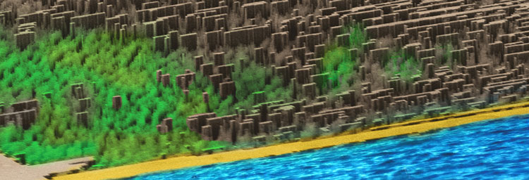
But Tokel hit upon another critical realization: Many practical components could be made out of self-organizing rod- or needle-like building blocks. These rod-like structures, generated due to the same nonlinear feedback effects that create the point-like modifications, also preserve a width of about 1µm for each block.
What’s more, these rods, which elongate along the direction of beam propagation, can be assembled to create a 2D layer, or even more complex 3D shapes, which can be created by scanning the laser beam over the chip.
“This is how in-chip optical devices, including holograms, gratings, lenses, microelements such as microfluidic channels or large-area-covering arrays are created,” said Tokel.
With this new capability, Tokel believes that he and his colleagues are at the point of conceiving a new way to realize a “lab-in-a-chip” system.
He added: “We can also imagine hybrid-systems, with in-chip photonics integrated to electronics and microfluidics parts, thus complementing them. These can incorporate waveguides for data transfer, holograms for diffractive optics, and other microparts to realize advanced biosensors, when coupled with meandering networks of channels.”

