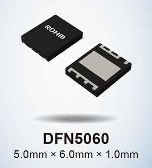
 ROHM 150V GaN HEMTs, GNE10xxTB series (GNE1040TB) increase the gate withstand voltage (rated gate-source voltage) to an industry-leading 8V – ideally to be applied in power supply circuits for industrial equipment such as base stations and data centers along with IoT communication devices.
In recent years – due to the rising demand for server systems in response to the growing number of IoT devices – improving power conversion efficiency and reducing size have become important social issues that require further advancements in the power device sector.
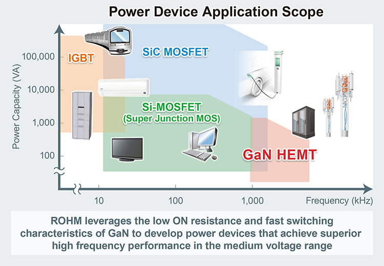
As GaN devices generally provide higher switching characteristics and lower ON resistance than silicon devices, they are expected to contribute to lower power consumption of various power supplies and greater miniaturization of peripheral components.
Along with mass-producing industry-leading SiC devices and feature-rich silicon devices, ROHM has developed GaN devices that achieve superior high frequency operation in the medium voltage range, allowing us to provide power solutions for a wider variety of applications.
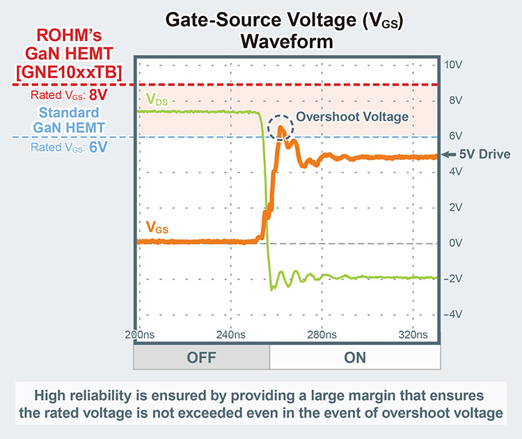
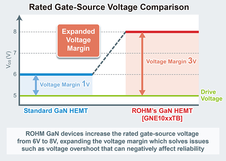
These new products utilize an original structure that raises the rated gate-source voltage from the conventional 6V to 8V. As a result, degradation is prevented, even if overshoot voltages exceeding 6V occurs during switching – contributing to improved design margin and higher reliability in power supply circuits. The GNE10xxTB series is offered in a highly versatile package featuring superior heat dissipation and large current capability, facilitating handling during the mounting process.
ROHM has trademarked GaN devices that contribute to greater energy conservation and miniaturization under the name EcoGaN™, and is working to expand the lineup with devices that improve performance. Going forward, ROHM will continue to develop control ICs that leverage analog power supply technology such as Nano Pulse Control™ and modules that incorporate these ICs, along with power solutions that contribute to a sustainable society by maximizing the performance of GaN devices.
Professor Masayoshi Yamamoto, Graduate School of Engineering, Nagoya University
This year, the Ministry of Economy, Trade, and Industry (METI) of Japan has set a target of 30% energy savings for new data centers by 2030 – less than 10 years from now. However, system performance must not only be energy efficient, but also robust and stable as they have become a vital part of our social infrastructure.
In response, ROHM has developed a new GaN device that provides a gate withstand voltage of 8V, the industry’s highest, providing a high degree of robustness and stability while achieving superior energy savings. Beginning with these products, ROHM will continue to improve power supply efficiency in power sources by combining with proprietary Nano Pulse Control™ analog power supply technology, creating a major technological trend that will help the semiconductor and telecommunications industries become carbon neutral by 2040.
What is EcoGaN™?
EcoGaN™ refer to GaN devices that contribute to energy conservation and miniaturization by maximizing the low ON resistance and high-speed switching characteristics of GaN, with the goals of reducing application power consumption, miniaturizing peripheral components, and reducing design load along with the number of parts required.
*EcoGaN™ is a trademark or registered trademark of ROHM Co., Ltd.
Key Features
1. Original structure extends the rated gate-source voltage to 8V
Existing GaN devices with a withstand voltage of 200V or less typically have a rated gate-source voltage of 6V with respect to a gate drive voltage of 5V, resulting in an extremely narrow voltage margin of just 1V. Exceeding the rated voltage can cause reliability problems such as degradation and destruction, plus the gate drive voltage requires high accuracy control, which has been a major obstacle to the popularization of GaN devices.
In response, this new series succeeds in raising the rated gate-source voltage from the typical 6V to an industry-leading 8V by adopting an original structure. This expands the voltage margin during device operation, so even if a voltage overshoot exceeding 6V occurs during switching, the device will not degrade, contributing to higher reliability of the power supply circuit.
2. Optimized package provides excellent heat dissipation and supports large currents
The GNE10xxTB series utilizes a highly versatile package with a proven track record for reliability and mountability that delivers superior heat dissipation and large current capability, facilitating handling during the mounting process. What’s more, using copper clip junction packaging technology reduces parasitic inductance by 55% over conventional packages, maximizing device performance when designing circuits for high frequency operation.
3. Achieves over 96.5% power supply efficiency in the high frequency band
These new products maximize device performance by increasing the rated gate-source voltage and adopting a low-inductance package, achieving a high efficiency of 96.5% or more in the high 1MHz frequency band, contributing to improved efficiency and greater miniaturization in power supply equipment.
Application Examples
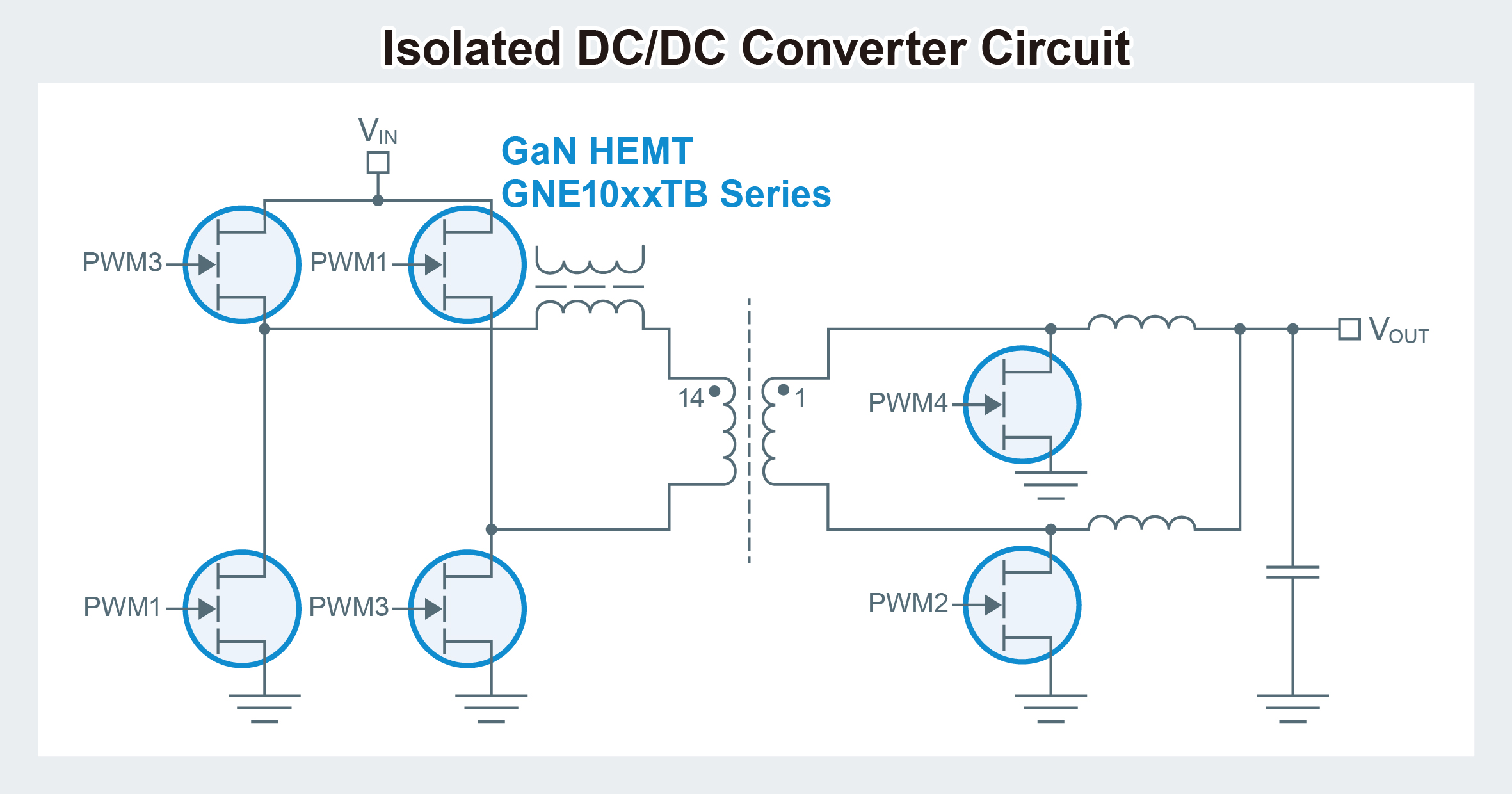
- 48V input buck converter circuits for data centers and base stations
- Boost converter circuits for the power amp block of base stations
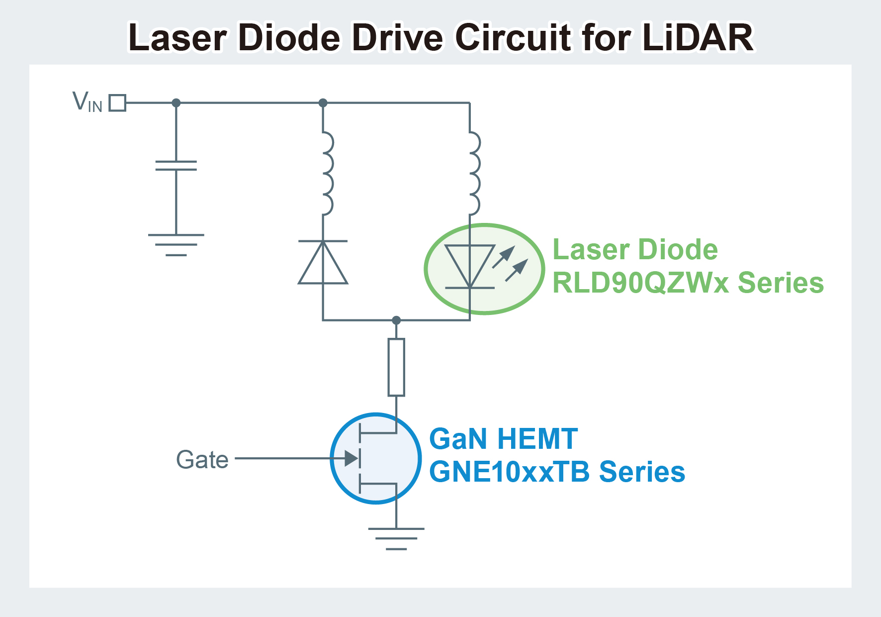
- LiDAR drive circuits, wireless charging circuits for portable devices
- Class D audio amps

Sample Circuits
Product Lineup
| Part No. | Drain-Source Voltage VDS [V] | Gate-Source Voltage VGS [V] | Drain-Source Current IDS[A] Tc=25ºC | Drain-Source ON Resistance RDS(ON) [mΩ] | Total Gate Charge Qg [nC] | Package [nm] |
|---|---|---|---|---|---|---|
GNE1040TB |
150 | 8 | 30 | 40 | 2.0 | DFN5060 [5.0×6.0x1.0] |
| ☆GNE1015TB | 55 | 15 | 4.9 | |||
| ☆GNE1007TB | 80 | 7 | 10.2 |
☆: Under Development
GaN Dedicated Web Page
https://pages.rohm.com/gan-technology.html
Terminology
Rated Gate-Source Voltage (Gate Withstand Voltage)
The maximum voltage that can be applied between the gate and source. The voltage required for operation is called the drive voltage, and when voltage above a threshold is applied the GaN HEMT is turned ON.
GaN HEMT
GaN (Gallium Nitride) is a compound semiconductor material used in next-generation power devices. It is beginning to see adoption due to its superior properties over silicon, such as excellent high-frequency characteristics. HEMT stands for High Electron Mobility Transistor.
Overshoot Voltage
A voltage that exceeds the specified voltage when switching ON/OFF.
Nano Pulse Control™
ROHM’s ultra-high-speed pulse control technology that achieves a switching ON time (control width of the power supply IC) on the order of nanoseconds (ns) in power supply ICs that makes it possible to convert from high to low voltages using a single IC – unlike conventional solutions requiring 2 or more power supply ICs.


![New Product [GNE1048TB] Power Supply Efficiency](https://www.rohm.com/documents/11303/9973405/060_GaN_EN_5.jpg/b7488910-cd8f-7c7e-4864-ae239837c25e?t=1646860163410)