Thermally Evaporated Environment-Friendly Semiconductors
As semiconductors gain greater functionality and production volume, the environmental cost also increases. The greenhouse gases and waste from the semiconductor manufacturing process are serious environmental issues.
A research team at the Department of Chemical Engineering at POSTECH developed a high-performance n-type semiconductor of Bi2S3 and a p-type Te semiconductor through simple thermal evaporation. The semiconductors can be grown over a large area using the process, which also manufactures the 8th generation large area OLED (2200 × 2500 mm) in driver circuits of OLED displays.
The team used a two-dimensional material, a transition metal chalcogen, like graphene. Compounds made of these metals have the properties of both conductors and semiconductors. They used Bi2S3 to manufacture the thin film of the semiconductor through a thermal evaporation process where they can control the quantity of electric charge through a simple thermal treatment, and semiconductors and conductors can be discretionally manufactured without doping.

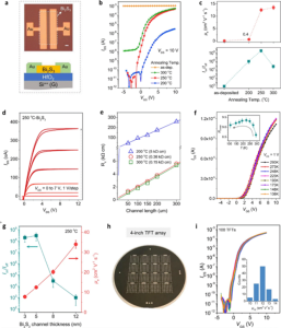
IMAGE: RESEARCH-RELATED FIGURES view more
Based on this process, they achieved a high-performance n-type thin film transistor and successfully developed a Te high-performance p-type semiconductor similarly. If manufacturers include this transistor and electronic circuit manufacturing process in the standard OLED manufacturing, they may manufacture the semiconductors through a single-step process. That will lower the high cost of manufacturing OLEDs, a disadvantage of the technology.

