Graphene is a unique form of carbon, consisting of a single layer of carbon atoms arranged in a neat honeycomb pattern. Recently, researchers at Florida State University discovered that twisting and layering graphene can change its ability to conduct electricity and interact with light. This study, published in Nano Letters, sheds new light on how graphene’s structure affects its performance.
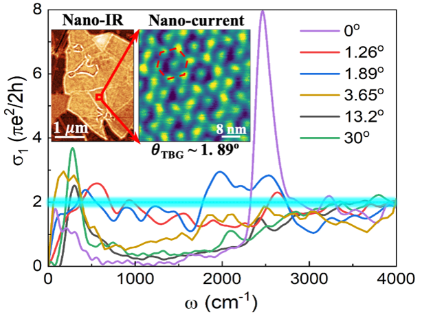
The team found that the conductivity of twisted bilayer graphene, for example, is not heavily impacted by physical or chemical manipulations but more on how the material’s minute geometry structure changes by interlayer twisting. To conduct the study, the team captured images of plasmons, tiny waves of energy that occur when electrons in a material move together, which appeared in various regions of the twisted bilayer graphene.
Using a specialized microscope, researchers were able to shine infrared light onto the graphene sample and capture images that reveal tiny energy waves, called plasmons. This microscope uses a needle to enhance how light interacts with the material, allowing scientists to see the plasmons in incredible detail.
They analyzed grain boundaries, or defects in the crystal structure, in the images to identify different regions of the twisted bilayer graphene. The areas containing the plasmons showed that the two sheets of carbon atoms were twisted at discrete angles in each, in addition to being twisted concerning a layer of hexagonal boron nitride. This transparent layered crystal was placed underneath.
When you layer two sheets of material and twist them, a “moiré pattern” appears—like when two patterned screens overlap. By twisting the graphene layers and placing them on a transparent crystal, researchers created a unique “double-moiré” pattern. This new layered structure is something researchers hadn’t explored in graphene studies before.

The team found that the optical conductivity of twisted bilayer graphene with boron nitride does not vary much with twist angle for angles of less than two degrees, even when the graphene is electrically doped and exposed to changing frequencies of infrared light. The optoelectronic properties of this super-moiré material are independent of chemical doping or the twisted bilayer graphene’s twist angle and depend more on the super-moiré structure itself and how it affects the electronic bands in the material, allowing for enhanced optical conductivity.
The team found the results exciting as they showed the potential of multilayer moiré systems in constructing materials with “on-demand” optical properties. The team’s findings indicate the significant impact of geometric relaxations in double-moiré lattices, showing how nanomaterials like graphene may respond to different manipulations. This can be used to produce such desirable optical properties as enhanced conductivity in a material, allowing for innovative advancements in moiré optoelectronics, including thermal imaging technologies and optical switching in computer processors.
So Here’s What You Don’t Know
- Twist Angle Matters: Twisting two graphene layers at specific angles, especially with a boron nitride layer, creates a “double-moiré” pattern. This superlattice changes graphene’s behavior, revealing stable new optical and conductive properties.
- Tunable Properties: Graphene’s optical and conductive abilities can be adjusted based on its structural geometry rather than relying solely on chemical changes. This opens up possibilities for materials with tailored characteristics.
- Potential for Advanced Tech: Engineers could use these findings to develop cutting-edge optoelectronic devices, like high-resolution imaging tools, enhanced optical switches, and efficient data processors that benefit from graphene’s adaptable properties.
Why it Matters
Understanding the unique properties of graphene and how they can be manipulated opens up exciting possibilities for engineers in fields ranging from electronics to materials science. The study’s findings on twisted bilayer graphene with boron nitride and its “double-moiré” structure reveal new avenues for designing materials with customizable optical and conductive properties. This means engineers could potentially develop components with tailored performance characteristics, ideal for next-gen optoelectronics. Applications such as high-resolution thermal imaging, optical switching, and enhanced data processing could see substantial improvements, thanks to the material’s unique response to geometric manipulation. By leveraging these properties, engineers can push the boundaries of what’s possible in device miniaturization, energy efficiency, and high-speed communication, setting the stage for advancements in everything from sensor technology to computing.
Original Story: Physics with a twist: FSU researchers publish new findings on graphene – Florida State University News

