World’s first vertically stacked GAA Si nanowire CMOS transistors
At this week’s IEEE IEDM conference, imec, reported for the first time the CMOS integration of vertically stacked Gate-All-Around (GAA) silicon nanowire MOSFETs. Key in the integration scheme is a dual-work-function metal gate enabling matched threshold voltages for the n- and p-type devices. Also, the impact of the new architecture on intrinsic ESD performance was studied, and an ESD protection diode is proposed. These breakthrough results advance the development of GAA nanowire MOSFETs, which promise to succeed FinFETs in future technology nodes.
GAA nanowire transistors are promising candidates to succeed FinFETs in 7nm and beyond technology nodes. They offer optimal electrostatic control, thereby enabling ultimate CMOS device scaling. In a horizontal configuration, they are a natural extension of today’s mainstream FinFET technology. In this configuration, the drive current per footprint can be maximized by vertically stacking multiple horizontal nanowires. Earlier this year, imec scientists demonstrated GAA FETs based on vertically stacked 8nm diameter Si nanowires. These devices showed excellent electrostatic control, but were fabricated for n- and p-FETs separately.
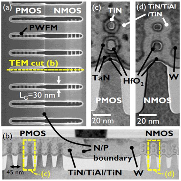
Imec now reports on the CMOS integration of vertically stacked GAA Si nanowire MOSFETs, with matched threshold voltages for n- and p-type devices*. Key in the integration scheme is the implementation of dual-work-function metal gates to set the threshold voltages of the n- and p-FETs independently. In this process step, p-type work function metal (PWFM) is deposited in the gate trenches of all devices, followed by selectively etching the PWFM down to the HfO2 from the n-FETs and subsequent deposition of the n-type work function metal. The observation of matched threshold voltages (VT,SAT = 0.35V) for nMOS and pMOS devices validates the dual-work-function metal integration scheme.
The impact of this new device architecture on the intrinsic ESD performance was investigated as well**. Two different ESD protection diodes have been proposed, i.e. a gate-structure defined diode (gated diode) and a shallow-trench isolation defined diode (STI diode). The STI diode was the better ESD protection device, showing an excellent ratio of failure current (It2) over parasitic capacitance (C). Measurements and TCAD simulations also prove that the ESD performance in GAA nanowire based diodes is maintained in comparison to bulk FinFET diodes.


Comments are closed, but trackbacks and pingbacks are open.